Samsung, TSMC Turn to Bigger Photomasks from ASML to Ease Global Chip Shortage
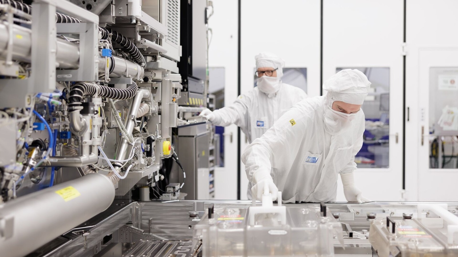
Samsung Electronics and Taiwan Semiconductor Manufacturing Co. (TSMC) have announced plans to incorporate ASML's newly sized photomasks into their production lines, a move intended to improve wafer yields and trim manufacturing expenses amid ongoing supply constraints.
The new photomasks, larger than the industry‑standard sizes currently in use, allow more circuitry to be printed onto each wafer in a single exposure. By increasing the number of functional chips per wafer, manufacturers can achieve higher throughput without expanding fab capacity, a critical advantage as the semiconductor sector grapples with persistent demand outpacing supply.
ASML, the Dutch lithography equipment supplier, has been developing the larger mask platform in collaboration with its biggest customers. The technology builds on the company's extreme ultraviolet (EUV) lithography systems, which already enable the production of chips at 5‑nanometer nodes and smaller. The expanded mask format is designed to work within existing EUV tool footprints, meaning fabs can adopt the upgrade without major retooling.
Both Samsung and TSMC see the upgrade as a practical response to the chip shortage that has affected industries ranging from automotive to consumer electronics since 2020. While new fab construction can take years and billions of dollars, improving yield on existing wafers offers a faster route to increasing effective output. Higher yields also translate into lower per‑chip costs, potentially easing price pressures that have been passed on to downstream manufacturers.
Industry analysts note that the shift toward larger photomasks aligns with a broader trend of incremental innovations aimed at squeezing more performance out of mature process nodes. As the market steadies, the ability to produce more chips per wafer could help stabilize inventories and reduce lead times for critical components such as processors, memory modules, and power management chips.
Looking ahead, Samsung and TSMC plan to begin pilot runs of the new masks later this year, with full‑scale deployment slated for 2025, contingent on successful validation. If the expected yield gains materialize, the approach could set a precedent for other fabs seeking cost‑effective ways to address supply gaps without the massive capital outlays required for new facilities. The collaboration underscores how equipment makers like ASML continue to play a pivotal role in shaping the semiconductor supply chain's resilience.


Comments (0)
Be the first to comment.
Join the discussion